Products
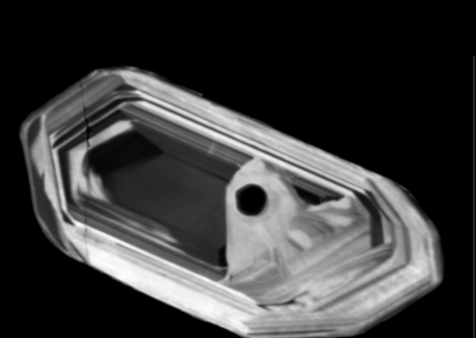
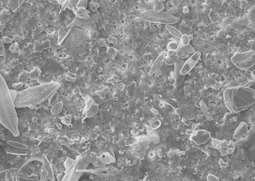
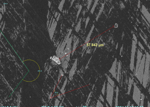
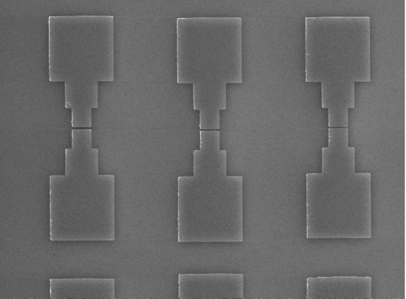
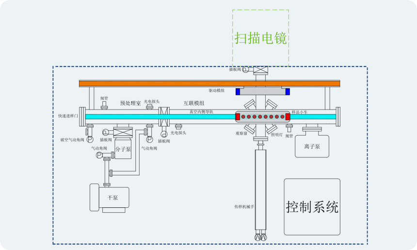
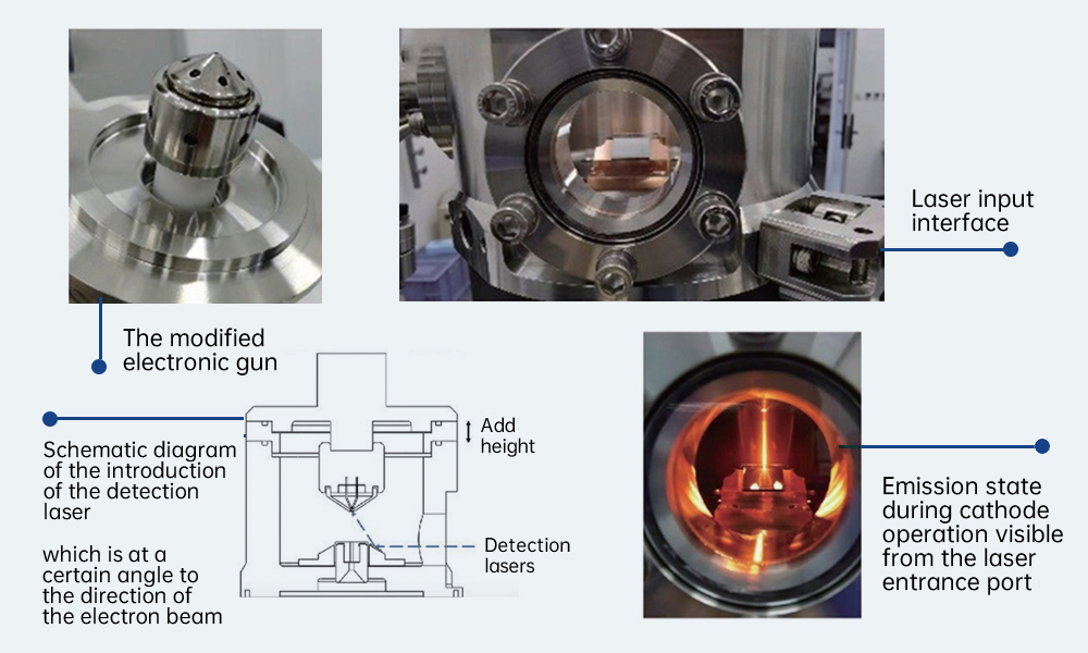
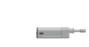
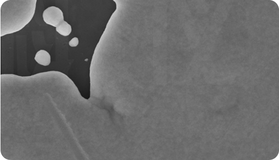
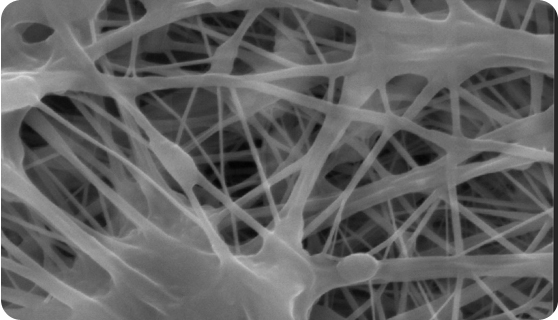
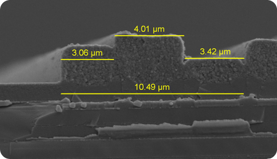
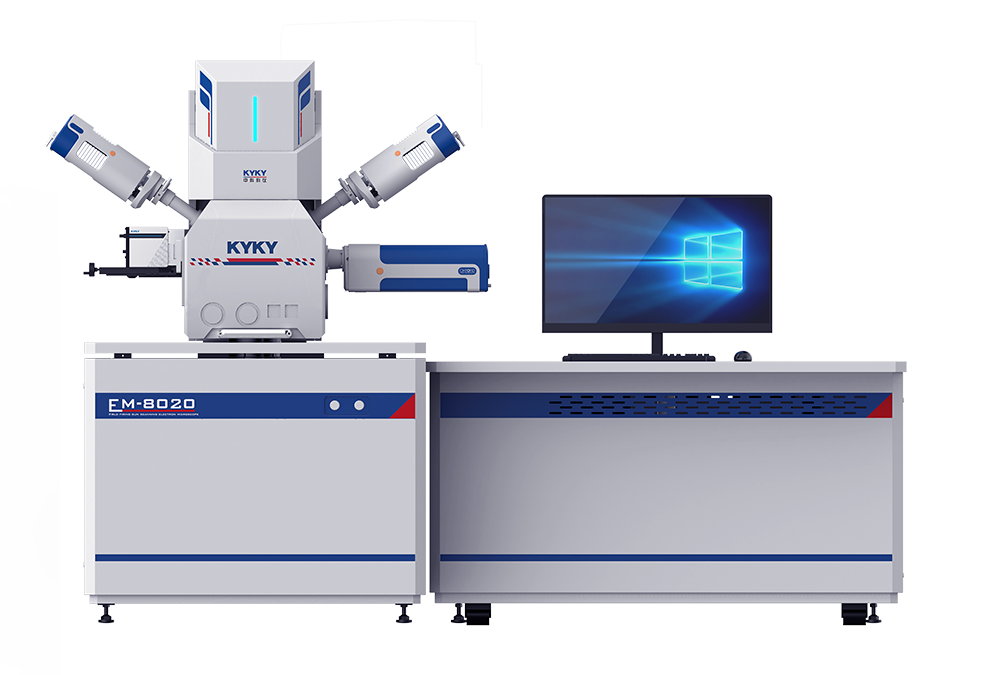
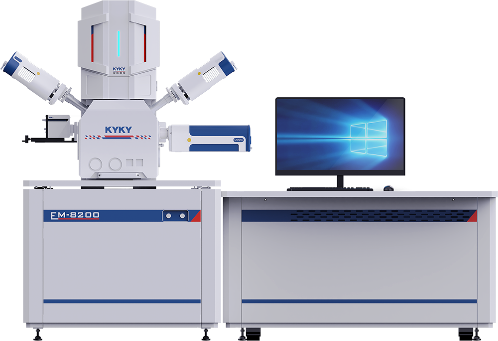
Field Emission Scanning Electron Microscope
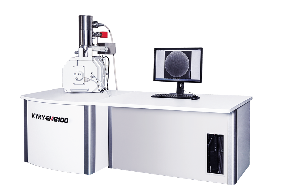
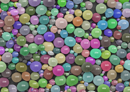
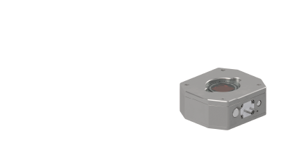
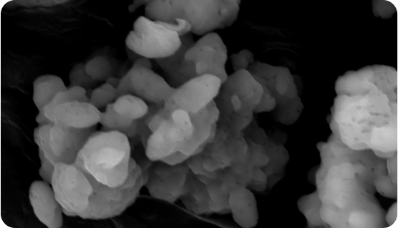
Tungsten Filament Scanning Electron Microscope
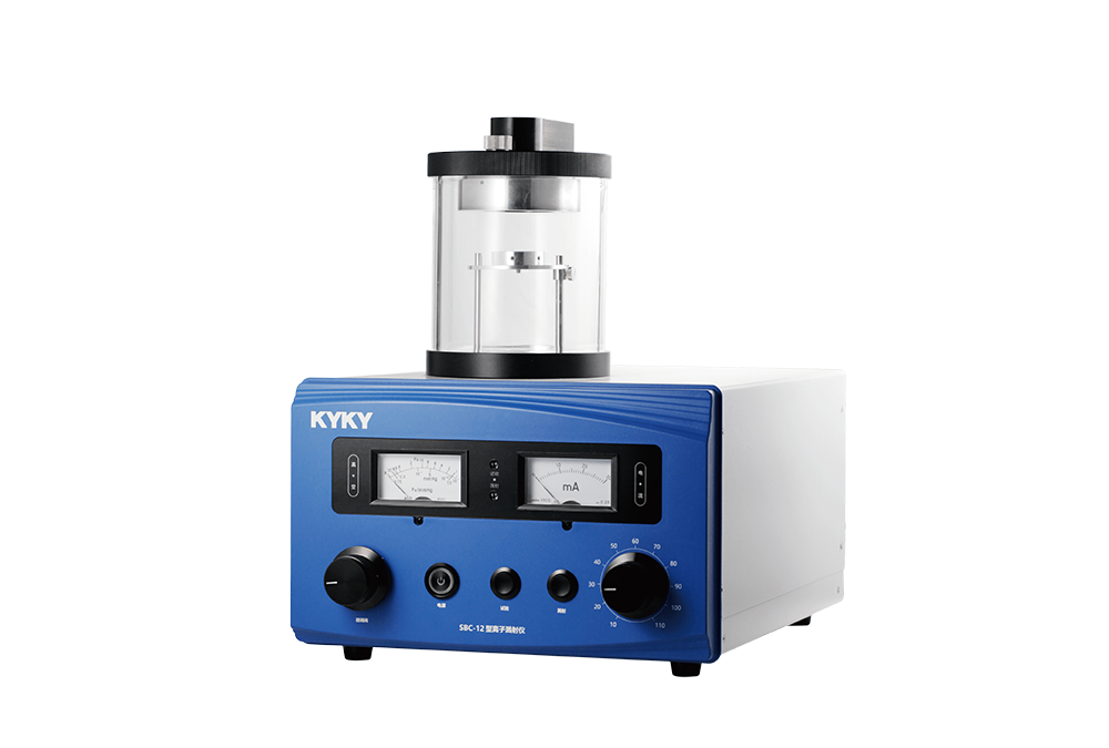
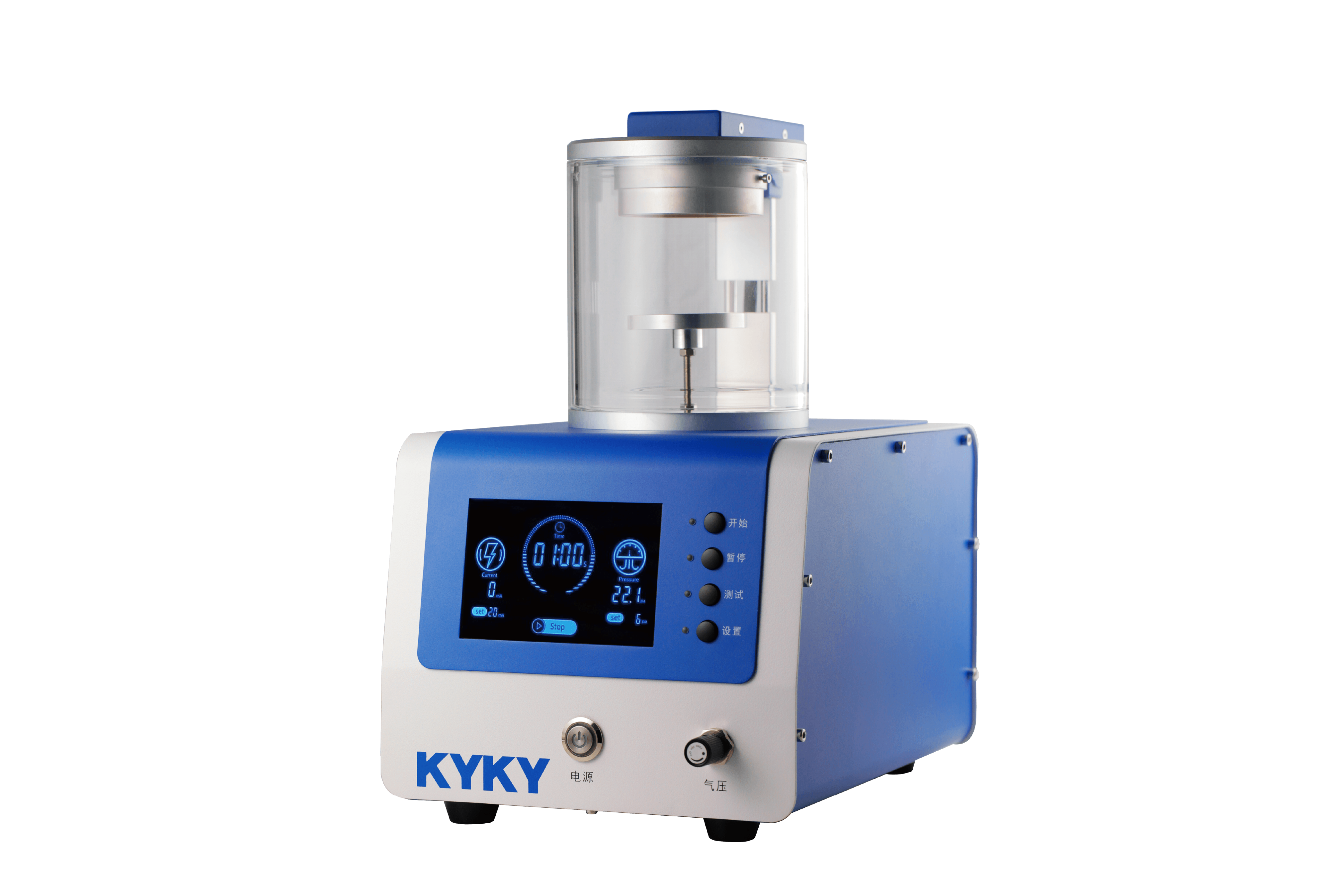
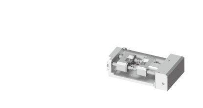
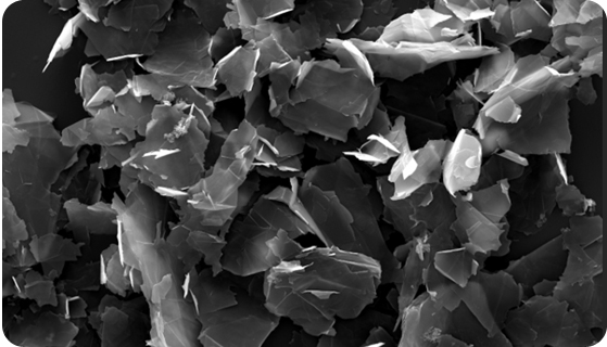
Ion Sputter Coater